The UCF researchers developed an alternative made from iron with phosphor dual-doped nickel selenide nanoporous film that in initial testing has demonstrated stability and long-duration capability which may prove to be an energy industry gamechanger.
In a July announcement from the University, Yang Yang, Associate Professor in the NanoScience Technology Center is quoted as stating, “This development will open a new window for efficiently producing clean hydrogen fuel from seawater.” He continues, “The seawater electrolysis performance achieved by the dual-doped film far surpasses those of the most recently reported, state-of-the-art electrolysis catalysts and meets the demanding requirements needed for practical application.” In a 200-hour test of the film, it held up producing hydrogen from seawater continuously. The film is not expensive to produce and is scalable for industrial applications.
The hydrogen produced using this nanofilm is classified as green. Electrolysis is the preferred route to go in producing hydrogen because there are zero emissions if the energy source is not fossil-fuel-based. That’s why the green hydrogen classification, as opposed to blue and grey hydrogen, is preferred.
If unfamiliar with these classifications of hydrogen fuels, blue hydrogen gets produced from fossil fuels when the resulting carbon emissions are captured and sequestered. Grey hydrogen produced from fossil fuels allows carbon emissions to get into the atmosphere. The fossil fuel industry, in its greenwashing efforts and to ensure continued profits from developing new fields to harvest, wants the public to buy into hydrogen produced from oil and gas.
In a world turning away from the burning of fossil fuels because of climate change, hydrogen from seawater would be a breakthrough of global significance. Hydrogen is ideal alternative energy for use in transportation, buildings, and homes where it can be used to recharge fuel cells or if compressed used for heating. Hydrogen, as opposed to natural gas, can be used by utilities in power plants as a backup or supplement to renewable energy generation from wind, solar, tidal and wave sources.
Yang’s research team’s expertise in advanced materials with application for use in renewable energy devices, environmental science, and smart electronics is focused on novel cutting-edge technologies that are much needed over this next decade in our fight to keep atmospheric warming from exceeding the 1.5-Celsius threshold established by the IPCC and Paris Climate Agreement and to stabilize the planet’s climate future.
]]>
Over 70 years ago, John Bardeen, Walter Brattain, and William Shockley sparked the semiconductor revolution with the fabrication of the first transistor. This fundamental technology now powers every aspect of science, innovation, and society. Projections put a $500 billion revenue tag on the semiconductor industry in 2018.
Nearly all products today rely on semiconductor materials science and its mightiest outcome, the transistor, which plays a decisive part in global computation, artificial intelligence (AI), and big data. The Economist magazine predicts that AI-related products and innovations will add nearly $16 trillion to GDP by 2030.
“Data to this century is what electricity was in….previous generations,” states Omkaram Nalamasu, Senior Vice President and Chief Technology Officer at Applied Materials. “Today, [we generate] something like 230 million tweets per day, 300 billion emails are sent per day, and about a hundred terabytes of data are loaded on Facebook every day. This pales in comparison to what is going to happen in the next five years. The data rate growth is about 80 percent.”
Worldwide data storage capacity is estimated to be around 6 zettabytes by 2020, each byte powered by semiconductor materials science. Exponential network and computation technologies including AI, the Internet of Things (IoT), the blockchain, autonomous vehicles, and the Internet itself are expected to generate orders of magnitude more data over the next five years than our current global storage capacity. The IoT network alone, projected to consist of over 50 million devices in 2020, will generate 600 zettabytes of information. That’s 100 times our current storage capacity of 6 zettabytes.
Once collected, how will we process and make sense of this data? The answer: advances in computational materials. It is materials breakthroughs, both in today’s semiconductor technologies and tomorrow’s quantum computers, that will be necessary to meet growing data storage and computation needs. That means breakthrough materials to manage it all. The exponential nature of Moore’s law, therefore, is converging with breakthroughs in materials discovery and production.
Traditional materials science involves costly, in-lab iteration and theory-based guesswork. But by harnessing the power of supercomputers, quantum mechanics, and importantly, machine learning, materials engineers will be able to do in hours what used to take weeks, months or years.
To contextualize this acceleration, let’s look at Thomas Edison’s invention of the light bulb. Edison required a bulb with low heat production, low power consumption, and a long-lasting, light-emitting material. With intuition and empirical data as his guide, Edison set out testing over 1,600 materials. After 14 months of testing and tinkering, he settled on a carbon-coated cotton thread. Fast forward 30 years to the introduction of the tungsten filament and the market for Edison’s carbonaceous-cotton filament is wiped out. So Edison’s 1,600 experiments and guesses produced what ultimately was a sub-optimal material solution that readily was replaced within three decades.
But today materials engineers can work with materials discovery software to analytically derive and virtually test optimal new materials for specified applications. “Materials engineering is the ability to detect a very small particle — something like a 10-nanometer particle on a 300-millimeter wafer,” explains Nalamasu. “That is really equivalent to finding an ant in the city of Seattle.”
Thanks to machine learning and exponential leaps in computation and quantum theory, the high price of guesswork involved in materials discovery is rapidly being phased out in favor of analytical and numerical methods. The materials scientist of tomorrow will be able to specify desired properties of materials and with basic processing parameters, and a quantum-computer based machine learning program, return the optimal material composition required for a specific application. And materials innovation will lead to exponentially more materials innovations. Remember: supercomputers (and soon quantum computers) are the lineage of the computational materials disruption that has been taking place over the past 70 years.
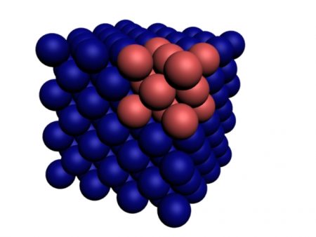
Think back to the state-of-the-art mobile phone in the 1980s, big, bulky, and reserved for Wall Street executives. Phones ran upwards of $4,000 and weighed over 5 kilos (a dozen pounds). These phones could only be used for calls and lacked any memory to store contact information. “If you were to build a smartphone in 1980,” Nalamasu explains, “that would cost something like $110 million. It would be about 14 meters [about 45 feet] tall, and it would require about 200 kilowatts of energy… that’s the power of materials engineering.”
Today, thanks to materials science breakthroughs in semiconductor technology, touchscreen displays, and batteries, children and executives alike can access smartphones with a 6+ inch Organic Light Emitting Diode (OLED) touchscreen displays, 256+ gigabytes of storage, integrated 1080 pixel cameras, and endless other features. By the end of 2018, we’ll have over 2.5 billion smartphones like what I have described above in use according to projections.

Now let’s extrapolate the user interface moment for mobile devices allowed by materials science breakthroughs to the current state of augmented reality (AR) and virtual reality (VR).
Today, bulky, expensive, and hard-to-use VR headsets dominate the industry. These headsets are ripe for precisely the same types of materials breakthroughs that enabled the rise of the smartphone from its ancestor the bulky mobile phone.
Some of the materials breakthroughs anticipated to come in and accelerate VR technology:
The future of AR and VR lies in sleek, slim, lightweight, and beautiful headsets that seamlessly integrate with our day-to-day lives. Thanks to coming materials advances, our future devices will be cheaper, thinner, faster and more powerful.
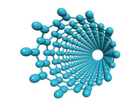
In its three main forms it serves different purposes. White phosphorus spontaneously ignites and is chemically extremely dangerous. It has been used in military applications in shells and grenades because it ignites with the air and creates smoke screens. When in contact with human skin or clothing it burns. It’s recent use in Israel’s conflict with Hamas in Gaza has raised considerable controversy.
Red phosphorus is relatively inert although it can revert to white when exposed to heat. You can find it as a coating on matchboxes and sandpaper. It is also used in flares and surprisingly as a flame retardant added to plastics used in electronics.
Black phosphorus is the least reactive and until recently had little commercial value. But nanoscience is altering our view of this material. In 2014 researchers created a field-effect transistor by assembling black phosphorus atoms into a two-dimensional puckered sheet. This seemed very promising if the black phosphorus could be manufactured in significant enough quantity, always the stumbling block.
But now a team of scientists, the same ones who created the field-effect transistor, have discovered a way to make black phosphorus nano-sheets in volume. This new capability is leading to all kinds of commercial applications including gas sensors, optical switches, and even as an additive in composite materials.
The method of manufacturing uses a liquid solvent, N-cyclohexyl-2-pyrrolidone (CHP) and acoustic waves to separate out black phosphorus atoms which are then filtered out using a centrifuge. The end product is nano-sheets in large quantities. The sheets oxidize if exposed to oxygen or water so the choice of CHP as a solvent is critical. it creates a protective shell around the nano-sheets giving them a much longer life.
In some applications black phosphorus is proving even better than graphene, another of the wonder nano-materials that are revolutionizing nano-electronics.
Some of the applications being explored include optical sensors and ammonia detectors.

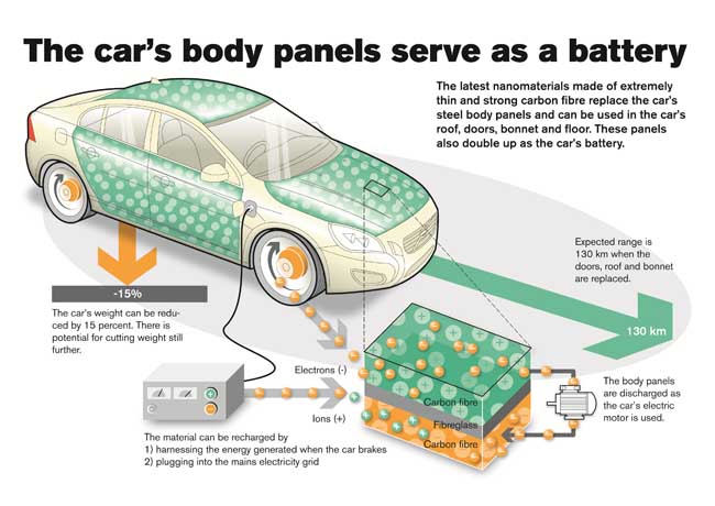
So Swedish automobile maker, Volvo (now owned by China’s Geely Holding Group) decided to dispense with the battery entirely, substituting a super capacitor made from advanced carbon fiber-based nano-materials that can be integrated into the body panels of the vehicle.
Volvo has chosen the S80 model to demonstrate this concept. The vehicles side body, doors, hood and roof panels are made of nano-material (see image below) that replaces the electric batteries used by conventional EVs. The vehicle plugs in to initially charge and then recharges the supercapacitor panels during braking. A single body panel like the hood can easily supply all the energy needed to run the vehicle’s internal electronics. Additional panels can power the drive train.
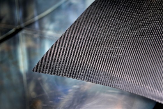
Volvo has yet to get beyond building a few of the panels but it is encouraged by early tests which show that the material stores energy much faster than conventional batteries. It also delivers its charge faster.
Integrating power storage into body panels is not a new idea. The Lola B12 69/E, an electric racing car that recently set a land speed record for EVs of 328 kilometers (204 miles) per hour, incorporates super capacitors and a fully-integrated drive train within the body of the vehicle.
The technology comes out of the Massachusetts Institute of Technology and Harvard University. Called nucleic acid origami, tiny particles consisting of DNA and RNA insert themselves into the genetic material of cancer cells turning off the genetic triggers that fuel their growth. Past research tried to deliver RNA and DNA material by combining it with other nanomaterials. But these technologies posed additional risk because the foreign carrier material for the RNA and DNA could lead to contraindications and health risks.

These new particles are made of DNA and RNA, and are biodegradable. They are designed to take advantage of a natural phenomenon in cells called RNA interference. Short interfering RNA or siRNA gets used by the body to disrupt genetic information carried from DNA to ribosomes within our cells. When DNA goes bad as in cancer cells, wouldn’t a disruptive agent be a welcome tool to stop the cancer from growing?
Nucleic acid origami allows researchers to create DNA packages combined with a single RNA strand that when injected can survive in the bloodstream and reach targeted tumor cells. Once delivered the nanoparticles can disrupt cancer cell growth at tumor sites and deal with rogue cancer cells that break off and migrate to other parts of the body.
The researchers are looking at using nucleic acid origami to deal with other diseases triggered by genes.
]]>Through mimicking nature we have made great technical strides. To the ones described above add another.
As reported in the journal, Smart Materials and Structures, Virginia Tech’s is Alex Villanueva has developed a robotic device that uses the propulsion and rowing actions of a jellyfish. His creation is Robojelly seen in the picture below.

Robojelly has one other characteristic that has significance for other types of robot designs, the ability to derive the energy to drive it from the surrounding environment. It does this using a platinum-based surface which catalyzes the hydrogen in seawater to create an exothermic reaction. The heat from the exothermic reaction makes Robojelly’s artificial muscles, called actuators, contract the bell-shaped dome expelling water to propel it forward.
The actuators are composed of nickel-titanium shape-memory alloy and sheets of carbon nanotubes coated with platinum powder. The material has been given the name BISMAC standing for Bio-Inspired Shape Memory Alloy Composites. The byproduct of the hydrogen reaction is water vapour.
Robojelly can run indefinitely deriving all the energy it needs from the seawater that surrounds it. Add a packet of sensors and it becomes a surveillance and telemetry tool that can measure and study the ocean without ever having to stop for fuel. To view Robojelly in action click here.
]]>


